Nanoscale self-organization at semiconductor surfaces

The growing tendency for the miniaturization of devices of everyday use, and the development of techniques and research methods for the characterization of the structural, chemical and electronic properties of nanometer systems, has caused an immense interest in nanotechnology and the science of advanced materials. Thus, the understanding of processes leading to the controlled modification of electronic and structural properties of solid surfaces at nanoscale are currently of major importance. Most semiconductor devices rely on special combinations of dissimilar materials to produce the desired electrical functions. A consequence of such combinations is that the component materials are rarely in thermodynamic equilibrium with each other. Therefore, reactions tend to occur at the interface separating adjacent materials/phases, which can result in reversion to the other equilibrium state, leading to the appearance of new structures of advanced properties.
Practically speaking, we distinguish two approaches that can be followed in the formation processes of systems with nanometer dimensions; these are called "top-down" and "bottom-up". The "top-down", is characterized by the fact that the resulting structure is produced by, for example, carving in larger objects in order to obtain a correspondingly smaller system with the given shapes. An example of such techniques being a whole group of lithographic methods. In turn, the "bottom-up" approach is a method based on using smaller components, even single atoms or molecules, to create larger systems. To obtain such ordered complexes with the given properties, various chemical and physical atom and molecule properties are used, which are the cause of self-organization phenomena.
In our experimental research we address the diversity of self-organization processes occurring at nanoscale in the following main thematic fields:
1) Self-organization processes of the metallic nanostructures on semiconductor surfaces
A. Growth of hexagonal gold (Au hcp) 3D nanostructures
Thermally induced self-organization of noble metal thin layers on the Ge(001) surface, carried out for specific experimental parameters, such as the heating and cooling rate, to create supported nanostructures of a hexagonal closest packed (hcp) crystallographic structure unusual for these metals. Gold is a noble metal and is an important material in various fields of science and technology such as nanoelectronics, catalysis and medicine. Gold crystallizes naturally in the face-centered cubic (fcc) phase, and its hexagonal closed packed (hcp) structure is a very rare and unusual form. By careful heat treatment and a controlled cooling in the thermally induced self-assembly processes of Gold on a Germanium surface at nanoscale the hcp phase of Gold (Au hcp) is synthesized in the form of stable 3D nanostructures. The phase diagram for the appearance of the Au hcp phase is experimentally defined together with the crystallographic structure of the Au hcp phase, as from electron microscopy measurements.
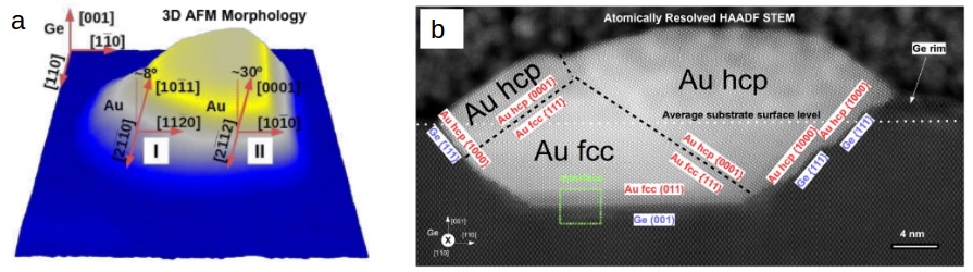
Hexagonal Gold (Au hcp) nanostructures, a) 3D AFM image, b) atomically resolved HAADF STEM image.
B.R. Jany, N.Gauquelin, T.Willhammar, M. Nikiel, K.H.W. van den Bos, A. Janas, K. Szajna, J.Verbeeck, S.Van Aert, G.Van Tendeloo & F. Krok, Controlled growth of hexagonal gold nanostructures during thermally induced self-assembling on Ge(001) surface, Sci. Rep. 7, 42420 (2017) doi:10.1038/srep42420
Au hcp (Hexagonal Gold) CIF structure file Crystallography Open Database COD 1545302
B. Self-organization processes of Au thin films on AIII-BV semiconductor surfaces
|
AIII-BV semiconductors as a result of their unique properties are being considered as a promising materials for the new generation of nanoscale electronic devices overcoming the limitations of Si based technology. One of the important aspects within AIII-BV semiconductor technology are the gold-semiconductor interactions which are responsible for the formation of the Metal-Semiconductor (M-S) junction which is a basic building block of almost all electronic devices. The control of the gold-semiconductor interaction via self-organization processes at the atomic level gives the possibility to control the M-S junction electronic properties. |
|
B.R. Jany, A. Janas, W. Piskorz, K. Szajna, A.P. Kryshtal, G. Cempura, P. Indyka, A. Kruk, A. Czyrska-Filemonowicz and F. Krok, Towards the Understanding of the Gold Interaction with AIII-BV Semiconductors at the Atomic Level, Nanoscale 12, 9067-9081 (2020) doi:10.1039/C9NR10256F
C. Thermally induced self-organization processes of Au films on a MoS2 surface
|
One of the most interesting features of atomic force microscopy is the possibility of manipulating nano-objects in a controlled way, which allows the investigation of fundamental physical properties such as friction and adhesion down to the nanometer scale and the fabrication of nanostructures with potential applications e.g. in molecular electronics as well. In this context 2D materials covered by metal clusters are a major target. With its layered structure, hexagonal symmetry and low friction coefficient, molybdenum disulfide (MoS2) is one of the most suited materials for nanomanipulation experiments. |
|
We have studied the frictional properties of selected triangular-shaped Au islands grown on a MoS2 surface, and investigated their pathways in a combination of AFM manipulation experiments and molecular dynamics simulations. The main novelty of this system is that the observed directions of motion are locked along the well-defined crystallographic orientations of the substrate, and the rotation of the islands are strongly hindered during sliding.
F. Trillitzsch, R. Guerra, A. Janas, N. Manini, F. Krok, E. Gnecco, Directional and angular locking in the driven motion of Au islands on MoS2, Physical Review. B, 2018 vol. 98 no. 16 doi:10.1103/PhysRevB.98.165417
2) Redox processes in transition metal oxides
Reduction-oxidation (redox) processes involve all reactions where the oxidation state of atoms changes. It requires the transfer of electrons between the species present in the system. When reduction occurs, the electron is gained (oxidation state decreases) and otherwise for oxidation. Redox processes happen all around us and can be treated as desirable (e.g. cellular respiration) or adverse (e.g. metal corrosion). In transition oxide materials the vast majority of the structural, chemical, and physical properties are governed by the oxygen concentration and, subsequently, by the cation oxidation state.
A. Electrical properties: work function, conductivity and resistive switching phenomena
|
As a result of redox processes, the oxygen content of the crystal changes, and thus the oxidation state of the transition metal, resulting in a change in the type of conductivity from semiconductor to metallic. Among other things, the resistive switching effect in these materials, which is used to produce memories (ReRAM) and a new neuromorphic architecture to simulate the operation of the human brain, is based on the redox processes. We study the reduction impact on electronic properties of the most important transition metal oxide crystals: TiO2, SrTiO3, BaTiO3, Nb2O5, and YSZ. In each case, the oxygen vacancy formation results in the emergence of new bandgap states and in an increase in the carrier concentration. This has a significant effect on surface conductivity and work function, which we measure by utilizing the state-of-the-art capabilities of UHV SPM techniques: local conductive AFM (LC-AFM, C-AFM) and Kelvin Probe Force Microscopy (KPFM, SKPM). |
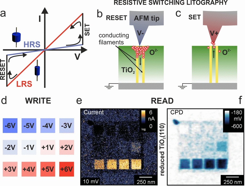 |
Our results confirm that a metal-to-insulator transition on the surface is connected with the preferential reduction of extended defects. Tuning the conductivity as well as the Fermi energy of metal oxides via reduction-oxidation could be directly used for VCM resistive switching, where oxygen vacancies migrate due to the external stimuli. Amongst all, we have proven that the surface of reduced TiO2 provides an excellent model system for nanoscale ReRaM memories with a cell size down to 25 nm.
D. Wrana, C. Rodenbücher, W. Bełza, K. Szot, F. Krok, In situ study of redox processes on the surface of SrTiO3 single crystals, Applied Surface Science, A 432 (2017) 46-52, doi.org/10.1016/j.apsusc.
B. New surfaces, interfaces and crystalline phases formation
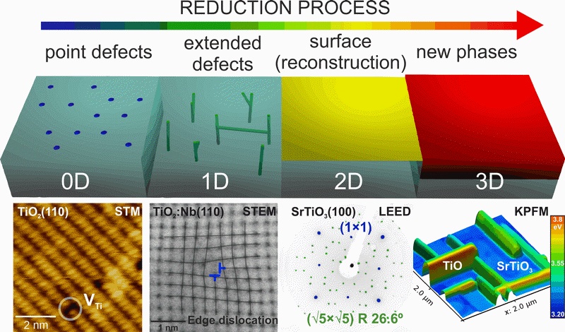
Redox processes enable the controllable formation of crystalline nanostructures with tailored oxygen nonstoichiometry, beginning from the single defects, through active surface reconstructions formation to the growth of exotic crystals with new stoichiometry. On the example of SrTiO3 (confirmed also for BaTiO3 and CaTiO3) we have presented that the use of an external getter, such as metallic titanium, enables the oxide decomposition via the incongruent sublimation of strontium. As a result, the surface becomes porous and heavily non-stoichiometric with an excess of Ti. This leads ultimately to the crystalline TiO nanowire formation on the surface of SrTiO3. We have proved that cubic TiO nanocrystals are virtually defect-free and have interesting interface properties, where two materials with the work function difference of almost 1 eV merge. Noteworthy, nanowires have persistent metallic conductivity, which is related to the connection to the dislocation network in the SrTiO3 matrix.
In published papers, we have presented a detailed explanation of the growth of nanowires, in terms of incongruent sublimation, crystallographic shearing and diffusion. In this way we have introduced the Extremely Low Oxygen Partial Pressure (ELOP) method, as an effective bottom-up method for the production of nanowires of reduced stoichiometry on perovskite surfaces.
D. Wrana, C. Rodenbücher, B.R. Jany, A.P. Kryshtal, G. Cempura, A. Kruk, P. Indyka, K. Szot and F. Krok, Bottom-up process of self-formation of highly conductive titanium oxide (TiO) nanowires on reduced SrTiO3, Nanoscale 11, 89-97 (2019) doi:10.1039/C8NR04545C
C. Optical and catalytic properties of reduced TiO2: the case of a single crystal vs. powder
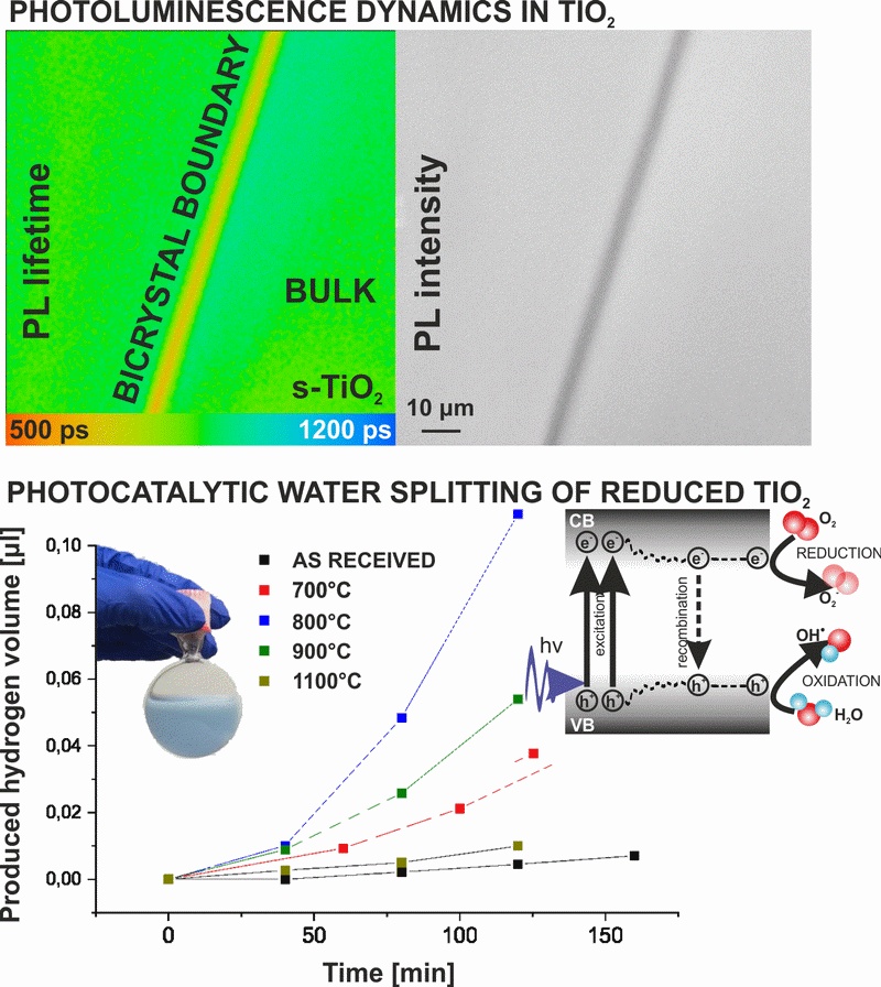
| TiO2 is not only one of the most efficient photocatalysts but it is also stable, cheap and safe for humans and the environment, as it has been used as a white pigment since ancient times. Within the main areas of interest are present-day photocatalytic water splitting and the degradation of pollutants. We focus on the idea that the efficiencies of reduction reactions could be improved by the defect engineering in oxides, helping to tune charge carriers' intensity and dynamics. We are investigating both single crystals and powder materials, in order to first show the basic principles of the reduction-oxidation influence on optical and catalytic properties and then directly test them. In particular, we distinguish the influence of defects of different dimensionality on the charge carrier dynamics, investigating 0D (oxygen vacancies and aliovalent dopants), 1D (dislocations) and 2D (grain boundaries) defects. Our results suggest that the reduction may help to enhance the photocatalytic behavior of real titanium oxide materials through increasing the photogenerated charge carriers’ lifetime. We observe a threefold increase of photoluminescence lifetime between nontreated rutile crystals and those that are heavily reduced. This correlates with the improved photocatalytic water splitting efficiency for titanium (IV) oxide powders reduced at temperatures of up to 900oC. |
|
C. Rodenbücher, D. Wrana, T. Gensch, F. Krok, C. Korte, & K. Szot (2020). The electronic properties of extended defects in SrTiO3—a case study of a real bicrystal boundary. Crystals, 10(8), 665. doi:10.3390/cryst10080665
3) Functionalization of transition metal oxide substrates for molecular electronic applications
A. Studies of the morphology and electronic properties of para-hexaphenyl structures grown on titanium dioxide
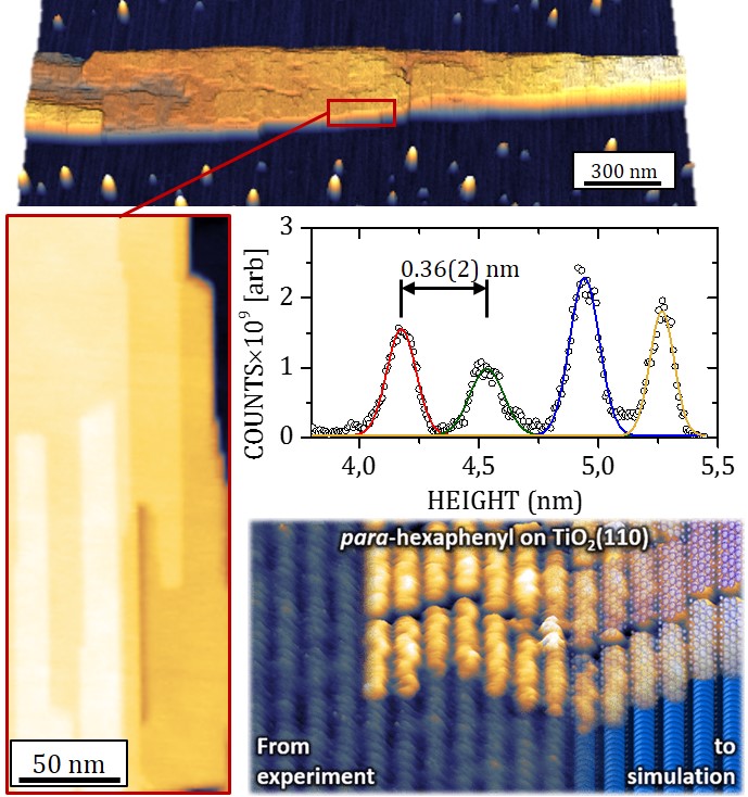
| Undertakings to improve the performance of organic semiconductor based electronic devices like organic field effect transistors (OFETs), organic light emitting diodes (OLEDs), and solar cells is at the same time an attempt to understand and control organic thin films. Especially, films composed of small, linear molecules like oligophenylenes (e.g. parahexaphenyl (6P)) have been shown to grow in a well ordered crystalline fashion. The relation between the structural properties of the organic thin films and their resulting electronic properties is the topic of ongoing research. To utilize these films in electronic and optoelectronic devices, the molecular orientation with respect to the substrate is crucial. In this respect, the surface quality of the substrate is an important factor for tailoring the electronic properties of the molecular nanostructures grown. Surface defects can effectively alter the molecule-surface interaction. The functionalization of the substrate surface with ion-beam-controlled alteration of the atomic step density (i.e. ripples) allows one to force variety growth modes in the molecules deposited. The various 6P molecular structures that are formed range from the formation of a wetting layer or less stable, two-dimensional lattice gas to needles, of flat-lying 6P molecules, or 6P islands of upright-standing molecules with significant elongation in the ripple direction. |
|
K. Szajna, M. Kratzer, W. Bełza, A. Hinaut, D. Wrana, T. Glatzel, C. Teichert, F. Krok, Initial stage of para-hexaphenyl thin-film growth controlled by the step structure of the ion-beam-modified TiO2(110) surface, The Journal of Physical Chemistry. C, 2019 vol. 123 no. 33, p. 20257-20269 doi:10.1021/acs.jpcc.9b03695
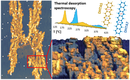
B. Influence of a permanent dipole moment on molecular structures’ growth process and their properties
|
Pentacene was a widely investigated molecule for its applications in organic electronics thanks to its properties. However, these properties are insufficient due to constant developments in this field. Pentacene derivatives are great candidates for research based on how extensively pentacene was investigated over the years. Therefore, in our research we also study dihydri-tetraaza-acenes (DHTA) as derivatives of pentacene and heptacene. These molecules contain a permanent dipole moment, which implies a stronger influence on materials' properties. We investigate the kinetics of growth processes and the electronic properties of the grown structures. |
|
4) Machine Learning and new methods of multidimensional data analysis
Machine Learning (ML) techniques which can analyze a huge amount of multidimensional data without any user interaction or bias, are successfully used in Electron Microscopy. Blind Source Separation (BSS) could be applied to hyperspectral SEM EDX data at nanoscale to overcome the limitations of SEM EDX to chemically quantify nanoobjects. Another example is the application of the ML Random Forest model for the atomically resolved HAADF STEM image chemical quantification, the ML successfully quantifies the image dealing with inherent noise. The ML techniques could be also successfully applied to fully automatic microscopic image analysis, which gives the possibility to analyze a large amount of image data collected during measurements sessions.
A. Overcoming the limitations of SEM EDX Chemical Quantification
By utilizing Machine Learning Blind Source Separation (BSS) analysis to simple and achievable SEM (Scanning Electron Microscopy) EDX (Energy Dispersive X-ray Spectroscopy) data collected at nanoscale followed by standard EDX ZAF, one can obtain a true chemical composition quantification from nanostructures. This provides unique possibilities to use simple SEM EDX in contrast to time consuming and costly TEM measurements of chemical composition quantification at nanoscale.
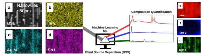
SEM EDX data collection at nanoscale in form of Spectrum Image (SI) maps from metallic nanowires a)-d), results of Machine Learning Blind Source Separation (BSS) by non-negative matrix factorization (NMF) e)-g), which separates EDX nanowires signal from background, this later is quantified by EDX ZAF.
B.R. Jany, A. Janas, and F. Krok, Retrieving the Quantitative Chemical Information at Nanoscale from Scanning Electron Microscope Energy Dispersive X-ray Measurements by Machine Learning, Nano Letters, Volume 17, Issue 11, 6507-7170 (2017) doi:10.1021/acs.nanolett.7b01789
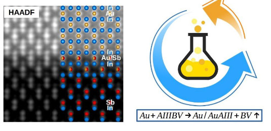
B. Machine Learning HAADF STEM image quantification
HAADF (High Angle Annular Dark Field) STEM (Scanning Transmission Electron Microscopy) image quantification is one of the techniques of the chemical composition quantification at the atomic level. Here, by way of an example, it was used for the Au/InSb system to distinguish between the columns containing Au atoms and the pure In–Sb columns (assuming a constant sample thickness). As a result of the noise inherent to the experiment, we used Machine Learning algorithms i.e. Random Forest which uses a multiple of decision trees which are trained on the subset of the experimental data (pure Au columns and pure In-Sb columns) from different areas of the same HAADF STEM image to classify (group into classes) the full dataset. The classified data come with a derived classification probability which is translated to the Au atomic concentration in the atomic columns. The derived Au concentration agrees with the true unknown Au concentration within the estimated experimentally relative uncertainty of the performed HAADF STEM chemical quantification as a result of the local sample thickness variation, which is 10.2%, and the estimated maximal relative uncertainty of the performed quantification related to the validity of the whole chemical quantification procedure, which is 12.6% (in comparison with the EDX measurements). HAADF STEM image quantification was performed using only free software ImageJ/FIJI together with Trainable Weka Segmentation.
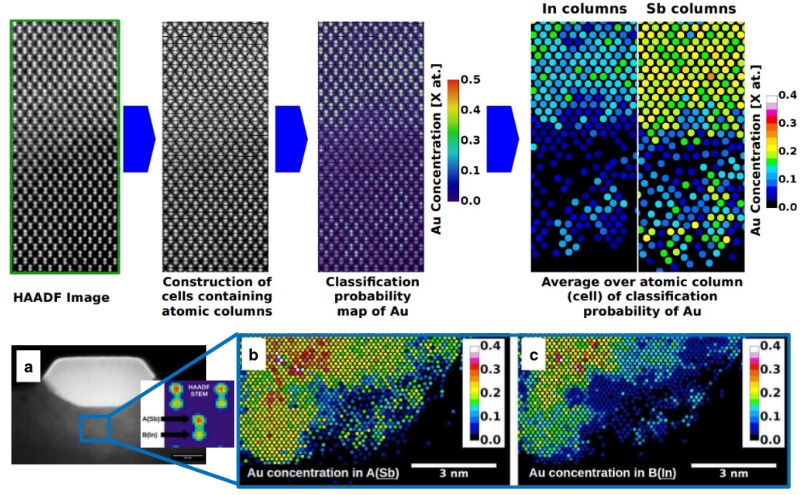
Machine Learning HAADF STEM image quantification of Au diffusion area formed in Au/InSb nanowires system a). The Au concentration was determined separatly for Sb and In atomic sublattice b)-c).
B.R. Jany, A. Janas, W. Piskorz, K. Szajna, A.P. Kryshtal, G. Cempura, P. Indyka, A. Kruk, A. Czyrska-Filemonowicz and F. Krok, Towards the Understanding of the Gold Interaction with AIII-BV Semiconductors at the Atomic Level, Nanoscale 12, 9067-9081 (2020) doi:10.1039/C9NR10256F
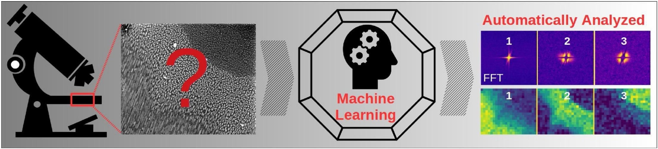
C. Automatic Microscopic Image Analysis
The analysis of microscopic images is a tedious job which requires patience and practice, usually performed by a microscopist following a measurement session. By using a method which utilizes moving window local Fourier Transform and Machine Learning blind decomposition of the data via Non-Negative Matrix Factorization (NMF), various microscopic images could be automatically analyzed. The method does not require any supercomputing and could be performed on a standard PC. It is also worth noting that our approach, in contrast to Neutral Network based approaches (e.g. Deep Learning), does not require any training datasets. This provides a unique possibility to analyze large amounts of image data, obtained during microscope measurement sessions, fully automatically within a reasonable time period and computing resources, therein saving the microscopist’s precious time. Our approach is freely available as a Python analysis notebook and Python program for batch processing.
B.R. Jany, A. Janas, F. Krok, Automatic microscopic image analysis by moving window local Fourier Transform and Machine Learning, Micron 130, 102800 (2020) doi:10.1016/j.micron.2019.102800
B.R. Jany, Python Jupyter Notebook to Perform Automatic Microscopic Image Analysis by Moving Window Local Fourier Transform and Machine Learning, Mendeley Data, v2 (2020) doi:10.17632/25x46xjyr5.2
Experimental techniques and methods used in these studies:
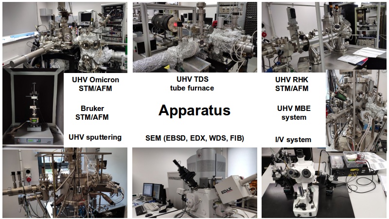
1. UHV-based SPM techniques: RT-STM/AFM Omicron NanoTechnology and VT-RHK system. Modes: contact and dynamic AFM, Kelvin Probe Force Microscopy (KPFM), Local-current AFM (LC-AFM), I/V spectroscopy
2. Ambient Bruker Multimode 8 microscope. Modes: contact and dynamic AFM, PeakForce, KPFM, LC-AFM
4. System for thin film growth with molecular beam epitaxy (MBE) and sputtering methods.
5. Electron beam characterization methods: Low Energy Electron Diffraction (LEED), Reflection High Energy Electron Diffraction (RHEED), Auger Electron Spectroscopy (AES)
6. Two-point probe electrical setup for resistive switching investigations
7. UHV system for powder samples preparation equipped with tube furnace and mass spectrometer
8. Quadrupole mass spectrometry (QMS), Temperature-Programmed Desorption (TPD).
9. Machine Learning tools
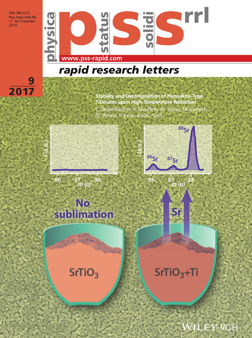
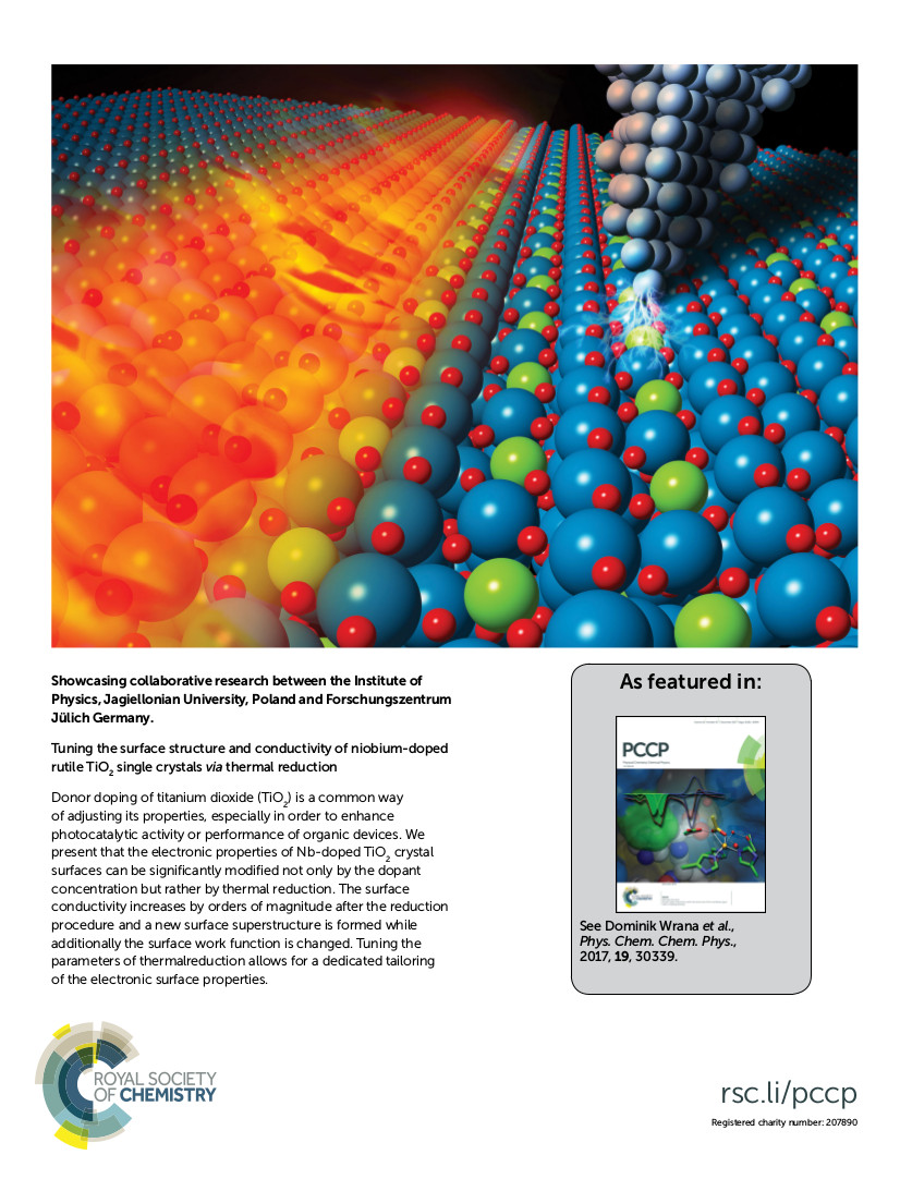
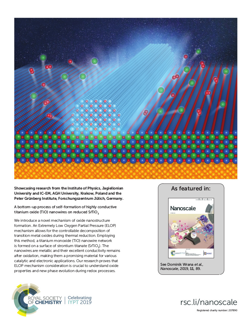
Magazine covers illustrating the results of our research
 |
 |
 |
 |
Group members
Group Head, room: D-1-38, phone: (+48)(12)(664)4632, email: franciszek.krok@uj.edu.pl
room: D-1-36, phone: (+48)(12)(664)4761, email: benedykt.jany@uj.edu.pl
- Dr Konrad Szajna
room: D-1-63, phone: +(48)(12)(664)4526, email: konrad.szajna@uj.edu.pl
- Dr Dominik Wrana
room: D-1-63, phone: +(48)(12)(664)4526, email: dominik.wrana@uj.edu.pl
- MSc Wojciech Belza
PhD Student, room: F-1-03, phone: +(48)(12)(664)4829, email: w.belza@doctoral.uj.edu.pl
- MSc Karol Cieslik
PhD Student, room: F-1-03, phone: +(48)(12)(664)4829, email: karol.cieslik@doctoral.uj.edu.pl
Publications
Self-organization processes of the metallic nanostructures on semiconductor surfaces
-
F. Krok, M.R. Kaspers, A. Bernhart, M. Nikiel, B.R. Jany, P. Indyka, M. Wojtaszek, M. Szymonski, R. Möller and C. A. Bobisch, Probing the electric transport on the reconstructed Au/Ge(001) surface with atomic resolution, Beilstein Journal of Nanotechnology 5, 1463–1471 (2014)
-
B. R. Jany, K. Szajna, M. Nikiel, D. Wrana, E. Trynkiewicz, R. Pedrys, F. Krok, Energy dependence of nanopillars formation on InSb semiconductorsurfaces under gallium FIB and noble gas ions beam irradiation, Applied Surface Science 327, 86–92 (2015)
-
M. Nikiel, B. R. Jany, D. Wrana, K. Szajna, F. Krok, SEM studies of vacuum conditions influence on thermally induced Au selforganization on Ge(001) surface, Surface and Coating Technology 277, 165–169 (2015).
-
M. Nikiel, B. R. Jany, D. Wrana, K. Szajna, A. Janas, R. Kozubski, F. Krok, Dynamics of thermally induced assembling of Au nanoislands from thin Au layer on Ge(001), CrystEngComm, 18, 5674–5680 (2016).
-
B.R. Jany, N. Gauquelin, T. Willhammar, M. Nikiel, K.H.W. van den Bos, A. Janas, K. Szajna, J. Verbeeck, S. Van Aert, G. Van Tendeloo, F. Krok, Controlled growth of hexagonal gold nanostructures during self-assembling on Ge(001) surface, Scientific Reports 7, 42420 (2017).
-
Elzbieta Trynkiewicz, Benedykt R. Jany, Dominik Wrana, Franciszek Krok, Thermally controlled growth of surface nanostructures on ion-modified AIII-BV semiconductor crystals, Applied Surface Science 427, 349–356 (2018). http://dx.doi.org/10.1016/j.apsusc.2017.08.240
-
E. Trynkiewicz, B. R. Jany, A. Janas, F. Krok, Recent developments in ion beam-induced nanostructures on AIII-BV compound semiconductors, J. Phys.: Condens. Matter 30 304005 (2018). https://doi.org/10.1088/1361-648X/aacc45
-
F. Trillitzsch, R. Guerra, A. Janas, N. Manini, F. Krok and E. Gnecco, Directional and Angular Locking in the Driven Motion of Au Islands on MoS2, Phys. Rev. B 98, 165417 (2018).
-
A. Janas, B.R. Jany, K. Szajna, A. Kryshtal, G. Cempura, A. Kruk, F. Krok, Nanostructure phase and interface engineering via controlled Au selfassembly on GaAs(001) surface, Appl. Surf. Sci. 492, 703–710 (2019) https://doi.org/10.1016/j.apsusc.2019.06.20
-
F. Trillitzsch, A. Janas, A. Özogul, C. Neumann, A. George, B. R. Jany, F. Krok, A. Turchanin, E. Gnecco, Scanning-Probe-Induced Assembling of Gold Striations on Mono- and Bi-Layered MoS2 on SiO2, MRS Advances, 1-7, (2020). doi:10.1557/adv.2020.151
-
B.R. Jany, A. Janas, K. Szajna, O. Kryshtal, G. Cempura, A. Kruk, A. Czyrska-Filemonowicz, F. Krok, Chemically driven growth of Au rich nanostructures on AIII-BV semiconductor surfaces, Nanoscale (2020), 12, 9067-9081, DOI: 10.1039/c9nr10256f.
Redox processes in transition metal oxides
-
D. Wrana, C. Rodenbucher, M. Krawiec, B. R. Jany, J. Rysz, M. Ermrich, K. Szot and F. Krok, Tuning the surface structure and conductivity of niobium-doped rutile TiO2 single crystals via thermal reduction, Phys. Chem. Chem. Phys., 19, 30339-30350 (2017) DOI: 10.1039/c7cp03136j
-
Christian Rodenbücher, Paul Meuffels, Wolfgang Speier, Martin Ermrich, Dominik Wrana, Franciszek Krok, and Kristof Szot, Stability and Decomposition of Perovskite-Type Titanates upon High-Temperature Reduction, Phys. Status Solidi- RAPID RESEARCH LETTER 11, 1700222 (2017). DOI: 10.1002/pssr.201700222
-
D. Wrana, C. Rodenbücher, W. Belza, K. Szot, F. Krok, In situ study of redox processes on the surface of SrTiO3 single crystals, Applied Surface Science, 432, 46–52 (2018). https://doi.org/10.1016/j.apsusc.2017.06.272
-
C. Rodenbücher, G. Bihlmayer, W. Speier, J. Kubacki, M. Wojtyniak, M. Rogala, D. Wrana, F. Krok, K. Szot, Local surface conductivity of memristive oxides mapped with true atomic resolution, Nanoscale, 10, 11498 (2018). DOI: 10.1039/c8nr02562b
-
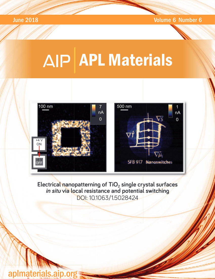
C. Rodenbücher, D. Wrana, P. Meuffels, M. Rogala, F. Krok, K.Szot, Electrical nanopatterning of TiO2 single crystal surfaces in situ via local resistance and potential switching, APL Materials 6, 066105 (2018). doi: 10.1063/1.5028424
-
D. Wrana, C. Rodenbücher, B. Jany, O. Kryshtal, G. Cempura, A. Kruk, P. Indyka, K. Szot, F. Krok, A bottom-up process of self-formation of highly conductive titanium oxide (TiO) nanowires on reduced SrTiO3, Nanoscale 11, 89-97 (2019) doi:10.1039/C8NR04545C
-
Christian Rodenbücher, Stephan Menzel, Dominik Wrana, Thomas Gensch, Carsten Korte, Franciszek Krok, and Kristof Szot, Current channeling along of extended defects during electroreduction of SrTiO3, Scientific Reports 9, 2502 (2019), https://doi.org/10.1038/s41598-019-39372-2
-
Dominik Wrana, Karol Cieślik, Wojciech Belza, Christian Rodenbücher, Krzysztof Szot and Franciszek Krok, Kelvin probe force microscopy work function characterization of transition metal oxide crystals under ongoing reduction and oxidation, Beilstein J. Nanotechnol. 10, 1596–1607 (2019). doi:10.3762/bjnano.10.155
-
M. Rogala, G. Bihlmayer, P. Dabrowski, C. Rodenbücher, D. Wrana, F. Krok, Z. Klusek and K. Szot, Self-reduction of the native TiO2 (110) surface during cooling after thermal annealing – in-operando investigations, Scientific Reports 9:12563 (2019) https://doi.org/10.1038/s41598-019-48837-3
-
C. Rodenbücher, K. Szot, D. Wrana, B. Jany, F. Krok, C. Korte, Localized electrochemical redox reactions in yttria stabilized zirconia single crystals, Journal of Physics: Energy (2020)
-
Christian Rodenbücher, Dominik Wrana, Thomas Gensch, Franciszek Krok, Carsten Korte and Krzysztof Szot, The Electronic Properties of Extended Defects in SrTiO3—A Case Study of a Real Bicrystal Boundary, Crystals 2020, 10(8), 665; https://doi.org/10.3390/cryst10080665
-
Rodenbücher, C., Bittkau, K., Bihlmayer, G. et al. Mapping the conducting channels formed along extended defects in SrTiO3 by means of scanning near-field optical microscopy. Sci Rep 10, 17763 (2020). https://doi.org/10.1038/s41598-020-74645-1
Functionalization of transition metal oxide surfaces for molecular electronic applications
-
M. Kratzer, D. Wrana, K. Szajna, F. Krok and C. Teichert, Island shape anisotropy in organic thin film growth induced by ion-beam irradiated rippled surfaces, Phys. Chem. Chem. Phys. 16, 26112 (2014)
-
D. Wrana, M. Kratzer, K. Szajna, M. Nikiel, B. R. Jany, M. Korzekwa, Ch. Teichert, and F. Krok, Growth of para-Hexaphenyl Thin Films on Flat, Atomically Clean versus Air-Passivated TiO2(110) Surfaces, J. Phys. Chem. C, 119, 17004−17015 (2015) DOI: 10.1021/acs.jpcc.5b04384
-
K. Szajna, M. Kratzer, D. Wrana, C. Menucci, B. R. Jany, F. Buatier de Mongeot, C. Teichert and F. Krok, Influence of TiO2(110) surface roughness on growth and stability of thin organic films, The Journal of Chemical Physics 145, 144703 (2016).
-
M. Kratzer, K. Szajna, D. Wrana, W. Belza, F. Krok, C. Teichert, Fabrication of ion bombardment induced rippled TiO2 surfaces to influence subsequent organic thin film growth, J. Phys.: Condens. Matter 30, 283001 (2018) https://doi.org/10.1088/1361-648X/aac758
-
K. Szajna, M. Kratzer, W. Belza, A. Hinaut, D. Wrana, T. Glatzel, C. Teichert, and F. Krok Initial Stage of para-Hexaphenyl Thin-Film Growth Controlled by the Step Structure of the Ion-Beam-Modified TiO2(110) Surface, J. Phys. Chem. C 123, 20257−20269 (2019), DOI: 10.1021/acs.jpcc.9b03695
-
W. Belza, K. Szajna, M. Kratzer, K. Cieślik, D. Wrana, M. Krawiec, C. Teichert and F. Krok, The molecular arrangement of para-hexaphenyl wetting layer on TiO2(110), J. Phys. Chem. C, 124, 5681−5689 (2020), https://dx.doi.org/10.1021/acs.jpcc.9b11533
Machine Learning and new methods of multidimensional data analysis
-
B. R. Jany, A. Janas, and F. Krok, Retrieving the Quantitative Chemical Information at Nanoscale from Scanning Electron Microscope Energy Dispersive X‑ray Measurements by Machine Learning, Nano Lett. 17, 6520-6525 (2017) DOI: 10.1021/acs.nanolett.7b01789
-
A. Janas, B.R. Jany, K. Szajna, A. Kryshtal, G. Cempura, A. Kruk, F. Krok, Nanostructure phase and interface engineering via controlled Au selfassembly on GaAs(001) surface, Appl. Surf. Sci. 492, 703–710 (2019) https://doi.org/10.1016/j.apsusc.2019.06.20
-
B.R. Jany, A. Janas, K. Szajna, O. Kryshtal, G. Cempura, A. Kruk, A. Czyrska-Filemonowicz, F. Krok, Chemically driven growth of Au rich nanostructures on AIII-BV semiconductor surfaces, Nanoscale (2020), 12, 9067-9081, DOI: 10.1039/c9nr10256f.
-
B. R. Jany, A. Janas and F. Krok, Automatic Microscopic Image Analysis by Moving Window Local Fourier Transform and Machine Learning, Micron 130, 102800 (2020), https://doi.org/10.1016/j.micron.2019.102800
Nanostructures Group Research Topics