
The Colorimetric Microscopy and Machine Learning Group
|
dr hab. Benedykt R. Jany, Ass. Prof. (group leader) |
The Colorimetric Microscopy and Machine Learning Group |
Aleksandra Szczupak (master student)
The group focuses on the understanding of the basic physical properties of the light-matter interaction at micro/nano scale on the surface manifested as a color appearance which is a consequence of the response of the electronic structure of the material. The research wants to show how color on a microscale level influences global color appearance. Diverse materials are studied like metals, thin films, gems, rocks etc. The research is carried out as part of basic research related to Color Science. To achieve these goals experimental methods like Colorimetric Microscopy (C-Microscopy) coupled with different methods of surface characterization like Scanning Electron Microscopy (SEM) Electron Backscatter Diffraction (EBSD) and Atomic Force Microscopy (AFM) are used.
Since the color appearance is a fundamental property of each material required by final consumers, the results of the research have a direct application in many different areas of industry and economy like metal processing, nanotechnology, packaging in food industry, arts and heritage, textile and fabrics industry and many more.
The research also focuses on the applications of advanced data analysis methods based of Machine Learning (ML) methods to experimentally collected microscopic images and hyperspectral data like:
- Automatic microscopic image analysis
- Hyperspectral Reflectance (R) data classification
- Machine Learning based HAADF STEM image quantification
- SEM EBSD 4D data analysis together with SEM EBSD Dictionary Based Indexing DI
- SEM EDX hyperspectral data analysis at nanoscale
- Atomically Resolved HAADF STEM Image Deconvolution
The research also includes Monte-Carlo modelling of Random Nucleation process on the surface for quantitative surface nucleation phenomena description.
The Laboratory of Colorimetric Microscopy (C-Microscopy Lab)
|
|

Colorimetric Microscopy (C-Microscopy) Approach - Quantifying Colors at Microscale

|
CIE 1931 chromaticity diagram |
Measured Hyperspectral Reflectance (R) (Colorimetrically reconstructed) of Unakite surface (metamorphic rock) at microscale. Results of C-Microscopy approach imaging. |


Colorimetric microscopy (C-Microscopy) approach is an experimental tool which can quantify color appearance of the surface at micro/nano scale. Different properties describing color in a quantitative way (i.e. dominant wavelength, excitation purity) as well as optical properties could be measured like Hyperspectral Reflectance (R) at microscale, which shows the response of the electronic structure of the material at microscale recorded in the form of reflectance spectrum (wavelength dependence of the reflectance) at each point.
Benedykt R. Jany, Quantifying Colors at Micrometer Scale by Colorimetric Microscopy (C-Microscopy) Approach, Micron 176, 103557 (2024) https://doi.org/10.1016/j.micron.2023.103557
Benedykt R. Jany. (2023). Python Jupyter Notebooks and Data for Colorimetric Microscopy (C-Microscopy) Approach. Zenodo. https://doi.org/10.5281/zenodo.7789585
Machine Learning (ML) and New Methods of Multidimensional Data Analysis in Microscopy
Machine Learning (ML) and Data Analysis techniques which can analyze a huge amount of multidimensional data without any user interaction or bias, are successfully used in different fields of Microscopy. Blind Source Separation (BSS) could be applied to hyperspectral SEM EDX data at nanoscale to overcome the limitations of SEM EDX to chemically quantify nanoobjects. Another example is the application of the ML Random Forest model for the atomically resolved HAADF STEM image chemical quantification, the ML successfully quantifies the image dealing with inherent noise. The ML techniques could be also successfully applied to fully automatic microscopic image analysis, which gives the possibility to analyze a large amount of image data collected during measurements sessions. The ML techniques are also well suited to the classiffication or Conductive AFM (C-AFM) data for the nano Metal-Semiconductor (M-S) Junction.
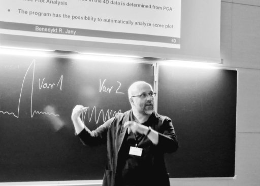
Invited lecture "Machining Learning Techniques in Electron Microscopy" on European School on Electron Microscopy and Tomography organized within the H2020-ESTEEM3 project. AGH, Krakow, Poland, 2022 (photo: A. Gruszczynski, AGH)
A. Overcoming the limitations of SEM EDX Chemical Quantification
By utilizing Machine Learning Blind Source Separation (BSS) analysis to simple and achievable SEM (Scanning Electron Microscopy) EDX (Energy Dispersive X-ray Spectroscopy) data collected at nanoscale followed by standard EDX ZAF, one can obtain a true chemical composition quantification from nanostructures. This provides unique possibilities to use simple SEM EDX in contrast to time consuming and costly TEM measurements of chemical composition quantification at nanoscale.
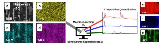
SEM EDX data collection at nanoscale in form of Spectrum Image (SI) maps from metallic nanowires a)-d), results of Machine Learning Blind Source Separation (BSS) by non-negative matrix factorization (NMF) e)-g), which separates EDX nanowires signal from background, this later is quantified by EDX ZAF.
B.R. Jany, A. Janas, and F. Krok, Retrieving the Quantitative Chemical Information at Nanoscale from Scanning Electron Microscope Energy Dispersive X-ray Measurements by Machine Learning, Nano Letters, Volume 17, Issue 11, 6507-7170 (2017) doi:10.1021/acs.nanolett.7b01789
B.R. Jany, A. Janas, and F. Krok, Collected Au/InSb and Au/Ge SEM EDX experimental data at Nanoscale as used in Retrieving the Quantitative Chemical Information at Nanoscale from Scanning Electron Microscope Energy Dispersive X-ray Measurements by Machine Learning (2017) doi:10.13140/RG.2.2.19558.93763
B. Machine Learning HAADF STEM Image Quantification
HAADF (High Angle Annular Dark Field) STEM (Scanning Transmission Electron Microscopy) image quantification is one of the techniques of the chemical composition quantification at the atomic level. Here, by way of an example, it was used for the Au/InSb system to distinguish between the columns containing Au atoms and the pure In–Sb columns (assuming a constant sample thickness). As a result of the noise inherent to the experiment, we used Machine Learning algorithms i.e. Random Forest which uses a multiple of decision trees which are trained on the subset of the experimental data (pure Au columns and pure In-Sb columns) from different areas of the same HAADF STEM image to classify (group into classes) the full dataset. The classified data come with a derived classification probability which is translated to the Au atomic concentration in the atomic columns. The derived Au concentration agrees with the true unknown Au concentration within the estimated experimentally relative uncertainty of the performed HAADF STEM chemical quantification as a result of the local sample thickness variation, which is 10.2%, and the estimated maximal relative uncertainty of the performed quantification related to the validity of the whole chemical quantification procedure, which is 12.6% (in comparison with the EDX measurements). HAADF STEM image quantification was performed using only free software ImageJ/FIJI together with Trainable Weka Segmentation.
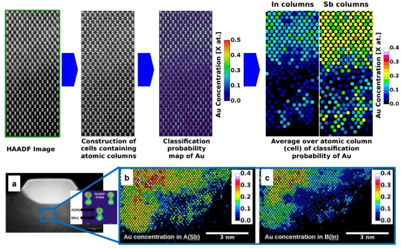
Machine Learning HAADF STEM image quantification of Au diffusion area formed in Au/InSb nanowires system a). The Au concentration was determined separatly for Sb and In atomic sublattice b)-c).
B.R. Jany, A. Janas, W. Piskorz, K. Szajna, A.P. Kryshtal, G. Cempura, P. Indyka, A. Kruk, A. Czyrska-Filemonowicz and F. Krok, Towards the Understanding of the Gold Interaction with AIII-BV Semiconductors at the Atomic Level, Nanoscale 12, 9067-9081 (2020) doi:10.1039/C9NR10256F
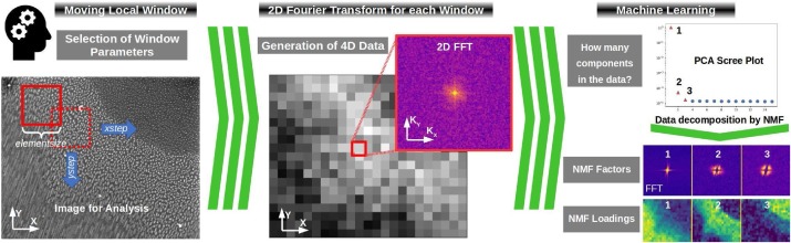
C. Automatic Microscopic Image Analysis
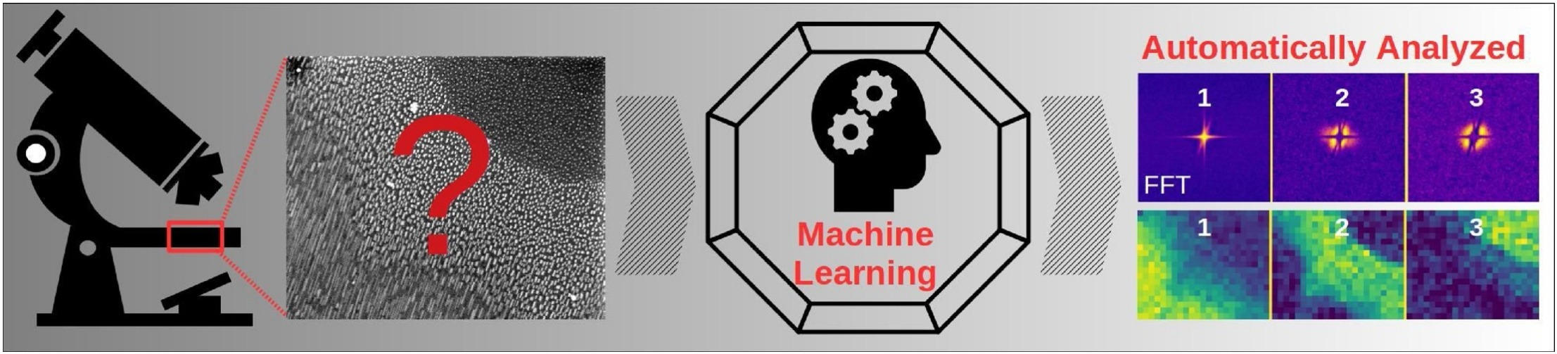
The analysis of microscopic images is a tedious job which requires patience and practice, usually performed by a microscopist following a measurement session. By using a method which utilizes moving window local Fourier Transform and Machine Learning blind decomposition of the data via Non-Negative Matrix Factorization (NMF), various microscopic images could be automatically analyzed. The method does not require any supercomputing and could be performed on a standard PC. It is also worth noting that our approach, in contrast to Neutral Network based approaches (e.g. Deep Learning), does not require any training datasets. This provides a unique possibility to analyze large amounts of image data, obtained during microscope measurement sessions, fully automatically within a reasonable time period and computing resources, therein saving the microscopist’s precious time. Our approach is freely available as a Python analysis notebook and Python program for batch processing.
B.R. Jany, A. Janas, F. Krok, Automatic microscopic image analysis by moving window local Fourier Transform and Machine Learning, Micron 130, 102800 (2020) doi:10.1016/j.micron.2019.102800
B.R. Jany, Python Jupyter Notebook to Perform Automatic Microscopic Image Analysis by Moving Window Local Fourier Transform and Machine Learning, Mendeley Data, v3 (2023) doi:10.17632/25x46xjyr5.3
D. Classification of Conductive AFM (C-AFM) data for nano Metal-Semiconductor (M-S) Junction
Using Machine Learning techniques one can classify Current-Voltage (I-V) measured for the nano Metal-Semiconductor (M-S) Junction using Conductive AFM (C-AFM). Usually at each point in nanoscale full current-voltage characteristics are recorded for the junction. The Machine Learning based classification allows for the identification of different conduction region for the junction (low, high conductivity regions). This later results in the extraction of map and corresponding I-V average spectra for the different conductivity regions. Machine Learning based classification simplifies the analysis, there is no need to analyze thousands of I-V spectra.

Machine Learning based classification of Conductive AFM (C-AFM) Current-Voltage (I-V) data for nano Metal-Semiconductor (M-S) Junction. Upper row: representation of I-V hyperspectral data as average current map together with AFM topography. Lower Row: Results of K-Means clustering of the data presented as a map of the clusters together with average I-V characteristics for each cluster. The analysis directly shows two conduction regimes for nano junction low conductivity and high conductivity.
A. Janas, W. Piskorz, A. Kryshtal, G. Cempura, W. Belza, A. Kruk, B.R. Jany, F. Krok, Into the origin of electrical conductivity for the metal–semiconductor junction at the atomic level, Applied Surface Science Volume 570, 150958 (2021) doi:10.1016/j.apsusc.2021.150958
E. Atomically Resolved HAADF STEM Image Deconvolution
The collected HAADF (High Angle Annular Dark Field) STEM (Scanning Transmission Electron Microscopy) images usually contain some form of blur due to the different experimental effects (source size, aberration, and other instabilities). The image deconvolution is successfully performed, to get rid of these effects and to increase the image resolution. The assumption of ideal microscope and ideal crystal lattice in the bulk is used i.e., the ideal crystal structure in the ideal microscope will be visible as points. The image resolution is increased making the interpretation of the structure easier.

A. Janas, W. Piskorz, A. Kryshtal, G. Cempura, W. Belza, A. Kruk, B.R. Jany, F. Krok, Into the origin of electrical conductivity for the metal–semiconductor junction at the atomic level, Applied Surface Science Volume 570, 150958 (2021) doi:10.1016/j.apsusc.2021.150958
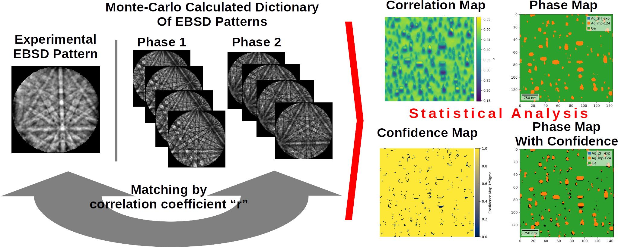
F. EBSD Dictionary Based Indexing (DI) - Phase Identification at Nanoscale
The SEM Electron Backscatter Diffraction (EBSD) Dictionary Based Indexing (DI) is a technique which uses a set of Monte-Carlo simulated EBSD diffraction patterns (Dictionary) to index the experimental collected diffraction. The indexing is done by comparing experimental patterns with a simulated one by comparing similarity metric for the patterns like correlation coefficient “r”. Tens of millions of comparisons are performed for single experimental pattern to find the final solution. The EBSD DI indexing is applied to the 4D EBSD data i.e., for each x,y pixel a 2D EBSD pattern is collected. By employing full statistical analysis to EBSD DI (full uncertainty analysis, statistical confidence maps) one can perform reliable Phase Identification for the structures at Nanoscale.
Benedykt R. Jany. (2023). Python Jupyter Notebook for Calculation of EBSD Dictionary Based Indexing (DI) Confidence Maps. Zenodo. https://doi.org/10.5281/zenodo.8117598
Applications of SEM EBSD to Nanostructures:
Ebru Cihan, Dirk Dietzel, Benedykt R. Jany, and André Schirmeisen, Effect of Amorphous-Crystalline Phase Transition on Superlubric Sliding, Phys. Rev. Lett. 130, 126205 (2023), doi:10.1103/PhysRevLett.130.126205
B.R. Jany, N.Gauquelin, T.Willhammar, M. Nikiel, K.H.W. van den Bos, A. Janas, K. Szajna, J.Verbeeck, S.Van Aert, G.Van Tendeloo & F. Krok, Controlled growth of hexagonal gold nanostructures during thermally induced self-assembling on Ge(001) surface, Sci. Rep. 7, 42420 (2017) doi:10.1038/srep42420
Monte-Carlo Modelling of Random Nucleation on the Surface
The Monte-Carlo modelling of a nucleation process on the surface can be used to extract the information on the nucleation character when compared with the experimental data. As the nearest neighbor distance between nucleating particles changes the character of the particles arrangement changes from clustering through the random nucleation up to regular arrangement. Comparing experimental data (SEM, AFM images of nucleating particles) with the results of Monte-Carlo simulation once can describe in a quantitative way the surface nucleation process.
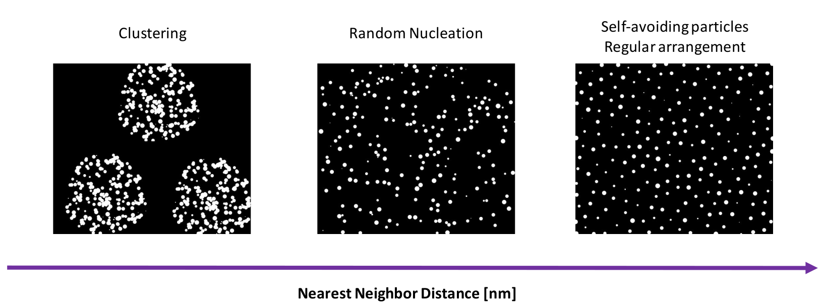
Results of Monte-Carlo modelling of a nucleation process on the surface dependent on nearest neighbor distance NND between the nucleating particles. As the nearest neighbor distance changes the character of the particles arrangement changes from clustering through the random nucleation up to regular arrangement.
Selected Publications
1. Benedykt R. Jany, Quantifying Colors at Micrometer Scale by Colorimetric Microscopy (C-Microscopy) Approach, Micron 176, 103557 (2024) doi:10.1016/j.micron.2023.103557
2. Ebru Cihan, Dirk Dietzel, Benedykt R. Jany, and André Schirmeisen, Effect of Amorphous-Crystalline Phase Transition on Superlubric Sliding, Physical Review Letters 130, 126205 (2023). doi:10.1103/PhysRevLett.130.126205
3. Gabriel L. Szabo, Benedykt R. Jany, Helmut Muckenhuber, Anna Niggas, Markus Lehner, Arkadiusz Janas, Paul S. Szabo, Ziyang Gan, Antony George, Andrey Turchanin, Franciszek Krok, Richard A. Wilhelm, Charge-State-Enhanced Ion Sputtering of Metallic Gold Nanoislands, Small 2023, 2207263 (2023). doi:10.1002/smll.202207263
4. A. Janas, W. Piskorz, A. Kryshtal, G. Cempura, W. Belza, A. Kruk, B.R. Jany, F. Krok, Into the origin of electrical conductivity for the metal–semiconductor junction at the atomic level, Applied Surface Science 570, 150958 (2021). doi:10.1016/j.apsusc.2021.150958
5. B.R. Jany, A. Janas, F. Krok, Automatic microscopic image analysis by moving window local Fourier Transform and Machine Learning, Micron 130, 102800 (2020). doi:10.1016/j.micron.2019.102800
6. Benedykt R. Jany, Arkadiusz Janas, Witold Piskorz, Konrad Szajna, Aleksandr P. Kryshtal, Grzegorz Cempura, Paulina Indyka, Adam Kruk, Aleksandra Czyrska-Filemonowicz and Franciszek Krok, Towards the Understanding of the Gold Interaction with AIII-BV Semiconductors at the Atomic Level, Nanoscale 12, 9067-9081 (2020). doi:10.1039/C9NR10256F
7. A. Janas, B.R. Jany, K. Szajna, A. Kryshtal, G. Cempura, A. Kruk, F. Krok, Nanostructure phase and interface engineering via controlled Au self-assembly on GaAs(001) surface, Applied Surface Science 492 703–710 (2019). doi:10.1016/j.apsusc.2019.06.204
8. B.R. Jany, N.Gauquelin, T.Willhammar, M. Nikiel, K.H.W. van den Bos, A. Janas, K. Szajna, J.Verbeeck, S.Van Aert, G.Van Tendeloo & F. Krok, Controlled growth of hexagonal gold nanostructures during thermally induced self-assembling on Ge(001) surface, Sci. Rep. 7, 42420 (2017). doi:10.1038/srep42420
9. Benedykt R. Jany, Arkadiusz Janas, and Franciszek Krok, Retrieving the Quantitative Chemical Information at Nanoscale from Scanning Electron Microscope Energy Dispersive X-ray Measurements by Machine Learning, Nano Letters, 17, Issue 11, 6507-7170 (2017). doi:10.13140/RG.2.2.19558.93763
10. Marek Nikiel, Benedykt R. Jany, Konrad Szajna, Dominik Wrana, Arkadiusz Janas, Rafal Kozubski and Franciszek Krok, Dynamics of thermally induced assembling of Au nanoislands from thin Au layer on Ge(001), CrystEngComm, 18, 5674, (2016). doi:10.1039/C6CE00471G
11. M. Nikiel, B.R. Jany, D. Wrana, K. Szajna, F. Krok, SEM studies of vacuum conditions influence on thermally induced Au selforganization on Ge(001) surface, Surface & Coatings Technology (2015). doi:10.1016/j.surfcoat.2015.07.031